
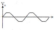
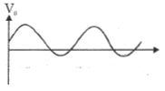
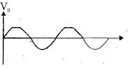
Consider the following circuit. The waveform given in input is as shown. If ${V_{B_1}}$ and ${V_{B_2}}$ are less than the peak value of the input,then the output will look like:
- A
- B
- C
- DNone of these.
Explore More
Similar Questions
The forbidden energy gap of $Ge$ is $0.75 \ eV$. The maximum wavelength of incident photon radiation that can generate an electron-hole pair in a $Ge$ semiconductor is ........... $\mathring{A}$.
Difficult
View SolutionIn a forward biased $p-n$ junction diode,the potential barrier in the depletion region will be of the form:
Medium
View SolutionWhen no bias is applied to a $P-N$ junction,the current is:
Easy
View SolutionFor the forward biased diode characteristics shown in the figure,the dynamic resistance at $I_{D} = 3 \, \text{mA}$ will be $..... \, \Omega$.
In the given figure,the voltage of point $A$ is ............ $V$.
Easy
View SolutionVedclass Products
For Students
Vedclass Test Series
Mock tests in real JEE/NEET style with performance analysis. 5-day free trial.
Start Free TrialFor Teachers
Exam Paper Generator
Generate Set A/B/C/D exam papers from 7.5L+ questions in 2 minutes. 3 chapters free.
Try FreeFor Institutes
Online Exam Module
Live online exams with unlimited students, 360° analytics & white-label branding.
See Demo